External Cavity Diode Laser - part 2: electronics
Introduction
In previous part I talked about optical part of ECDL controller. I mentioned requirements for tight control of temperature of all elements involved. In this part, we'll discuss what electronics is required to achieve that.
Requirements
- Millikelvin resolution measurement of temperature of both internal baseplate and laser diode
- Precise regulation of injection current
- Driving Peltier modules in heating and cooling mode with 16 bit resolution
- USB control
- simple power supply requirements
1. Precise thermometer
There are three main ways to measure temperature:
- using thermoelectric effect in thermocouple
- using semiconductor dependence on temperature, most often employed in integrated thermometers
- using thermoresistive effect in thermistor
Thermocouple signal is very low, so it's hard and expensive to design an amplifier with low enough internal noise to maintain mK resolution. What's more important, thermocouple effect happens on all material changes, which requires monitoring temperature of PCB and careful cable material choice. Integrated thermometers are very nice, with parts like DS18B20 providing 0.1K performance for extremely low price. Unfortunately, I was unable to find an integrated thermometer with mK resolution, much less accuracy. On the other hand, thermistors are well fitting components for this application. They have high change of resistance over temperature, which minimizes PCB's temperature influence and reduces issues with amplifier's noise. They're analog components, so resolution is, in theory, unlimited. One downside they have is high nonlinearity, which requires higher bit depth from the converter to maintain required resolution bit depth.
The signal path is composed of 3 main components:
- precise and stable 5VA reference - MAX6035
- operational amplifier providing gain to match wanted temperature range to full ADC range
- 16 bit, SAR ADC digitalizing signal
If the component selection seems a bit suboptimal, that's because it is. My auxiliary design goal here was to use as many components I already have, to burn through the pile of components left from other projects. My parts bin didn't include any sigma-delta converter.
To minimize influence of manufacturing tolerances, reduce need for calibration and desensitize the circuit to ambient temperature changes special 0.05%, 10ppm/K resistors are used in the feedback path and for input divider. During layout, attention was paid to keep them physically close together to be able to coat them with thermally conductive glue for further thermal coupling. The operational amplifier selected for the application also has to have minimal offset voltage, and it's temperature dependence.
 |
| schematic of thermistor amplifier and digitalizer |
Because of the extremely high sensitivity of this circuitry, it was important to consider unusual sources of interference. Piezoelectric effect is one of them. To eliminate coupling of mechanical vibrations to the circuit, special capacitors have to be used in the signal path. Ceramic capacitors can be made out of different dielectric materials. Low capacitances tend to be realized from C0G dielectric, while big ones from X5R or X7Y. While having smaller dielectric constant, C0G has many properties that make it favorable in electronic circuits, especially minimal piezoelectric effect. C_f symbolizes the biggest C0G capacitor available in package used, at the time of purchase it was 33nF.
In the end, if further resolution increases will be needed, there's an option to average results from ADC. The ADC can operate up to around 80 ksamples/s while temperature changes can be safely limited to 10 Hz bandwidth, giving, at least in theory, another 6.5 bits of resolution. For averaging to work optimally, input stage RMS noise should be around 1 LSB of the converter, currently it's much lower. If one wishes to enable averaging mode, 10k resistors in the feedback loop have to be increased to around 200k.
2. Injection current regulation
In contrary to most of the controller design, the laser diode driver isn't very precise. It's based on a simple op-amp current source driven by a digital to analog converter. The converter has resolution of 12 bit but 12 LSB INL. That means that while fine-tuning of output current is possible with high resolution, the absolute control of output current is possible with only 0.3% accuracy. To improve long term stability, DAC with external reference input was used with reference reused from thermistor section.
To reduce high frequency noise and scale signal, low pass filter was used (R27,R28,C28).
 |
| schematic of laser diode driver |
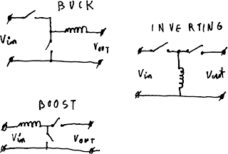
3. TEC drivers
Peltier drivers are really tricky part of this design. They need to provide high power, bipolar output with high efficiency while generating minimum disturbances to sensitive analog frontend nearby. The simplest solution would be based on class A or AB analog amplifier. Unfortunately the power loss in such stage can be unacceptably high and what's worse changing with load. That would double heat output in the worst case, making the passive radiator bigger and bulkier. Additionally, any temperature control loop would have to model how driver's power dissipation influences optics.
The final design is based on integrated H-bridge filtered by 2nd order symmetrical LC filter. To minimize size of the solution and common mode interference, a coupled inductor was used instead of the more classical two inductor solution. To further reduce required inductance and capacitance to manageable values, the highest switching frequency available in integrated H-bridges was used, 500 kHz. With 38.5uH inductance and 24 capacitors 10uF I got less than 0.5 mVpp ripple. To achieve this theoretical values, I had to pay a lot of care to the physical layout to make sure I don't introduce excessive ESR or ESL.
 |
| schematic of TEC driver |
 |
| layout of the filter section |
It's worth noting that rp2040 runs at clock speeds of up to 133Mhz, giving PWM resolution of just 266 steps. This is further reduced by minimum on and off time requirements of integrated H-bridge. This resolution is again much lower than required to implement a control loop capable of precise enough regulation.We can again use the fact that thermal response of the system is much lower and dither PWM values, but more on that next time!
5. USB control
To make the device as user accessible as possible, I opted to make the device fully programmable over USB. Both parameters and firmware can be updated over USB, with firmware in ROM stopping users from bricking the device. The firmware update uses rp2040 default USB bootloader, that shows up as a mass storage device. Configuration is set via SCPI over USB serial protocol (see wiki for detailed discussion).
6. power supply
rp2040 requires 3.3V power, a laser diode requires at least 8V to operate, Peltier modules require anything between 3V and 12V and screen operates between 11.5V and 12.5V. While In lab conditions, I could just use multiple power supplies, in order to make the device a bit more portable I opted for single power supply and onboard regulators for final design. Input power rail supplies screen, H bridges and laser diode driver directly, while 3.3V for rp2040 are generated using small, onboard switching regulator. In retrospect, I'd probably go for linear regulator as rp2040 consumes up to 40 mA, so the regulator would generate less than 400 mW of heat, but I already designed the converter for another project and had all parts available so why not use it.
If screen is used then input power is fixed at 12V, while without screen it can be anything between 6V and 16V. I expect the circuit to be used without onboard screen in most applications, giving the option to optimize the circuit for minimum noise or higher TEC power by changing supply voltage.
7. Closing remarks
While I'm happy with the overall design for next iteration, I'd introduce a few changes if there will ever be a next revision.
The controller will be open hardware when done. The device is far from finished, and as such I don't want to share any misinformation related to mistakes online. If you nevertheless would like to get all the sources, feel free to reach out to me.
Comments
Post a Comment